Tuesday 22 March 2011

The VU-Transmitter for 20m


K.P.S.Kang, VU20WF of the recently formed VU QRP Club has designed several club projects based upon very small printed circuit boards. The first of these that I saw and built was a transmitter based on the W6BOY Pixie. My version is much bigger than the original - for ease of building.

The drawing shows the circuit of the VU Transmitter. T1 is a Colpitts oscillator with C1 and C2 forming the capacitive feedback divider. The oscillator is crystal controlled but VC provides some useful frequency shift. VC can be a small variable capacitor or a trimmer. The maximum capacitance should be in the 50 to 75pF range. Larger values offer more shift but attempting to move the frequency too much will produce instability and eventually the oscillation will cease. The addition of an inductor of about 16uH will offer several kHz of frequency shift. (see VXO Option)

C3 couples the signal to the power amplifier, T2. The biasing resistor R5 controls the output of T2. Usually a value in the range 33K to 100K is suitable. The higher the value - the higher the output of T2. 47K is a useful starting value for experimentation. I suggest that T2 is not run higher than 1 watt of RF output power. It will get warm and a small star heatsink ought to be fitted.

The collector load for T2, RFC1, is a home made RF Choke. Carefully wind 12 turns of 38 swg (about 34 awg) enamelled copper wire (any small enough gauge will do) through a ferrite bead. RFC2 is a small 100uH axial choke which is essential when using T2 as the receiver mixer. It also provides a useful RF load on the input of T2 and increases the drive to T2. The transmitter output is coupled from the collector of T2 via C4 to a low pass filter.

http://www.southgatearc.org/qrp/transmitter.htm

15 METER VXO-TUNED CW TRANSMITTER


An easy-to-build and affordable CW rig that puts out about 500 milliwatts on15 meters, this simple modification of W7ZOI's classic two-stage "Universal QRP Transmitter" (also known as the "Little Joe" ) features a VXO circuit that "warps" each crystal frequency by as much as 10kHz or more for increased flexibility. This transmitter's oscillator runs throughout the transmit period; voltage is keyed to the amplifier section while the oscillator is on. After construction,tuneup is a snap: connect a 12-15 VDC power source and 50-ohm dummy load or RF wattmeter and tune a monitoring receiver to the anticipated transmit frequency. Flip on the oscillator switch and adjust C3 until a tone is heard on the receiver. Play with C1and notice the shifting of frequency (the crystal frequency DECREASES asC1's capacitance INCREASES). Depress the key and adjust C3 for maximum output. Tuneup adjustment is now complete. Hook up an appropriate antenna (a 40-meter dipole works great on 15 meters without use of a transmatch or antenna tuner)and there you go - bring on the sunspots!

Unless otherwise noted, decimal capacitance values are in microfarads(uF);

whole-number values are in picofarads (pF or uuF).

s.m.=silver mica.

* = see below.

http://boni.narod.ru/15xmtr.html

10-M DSB QRP TRANSMITTER WITH VFO


NE602 circuit : 10-M DSB QRP TRANSMITTER WITH VFO
NE602
NE602 circuit : 10-M DSB QRP TRANSMITTER WITH VFO
NE602
The three schematics represent three building blocks for a 10-meter SSB transmitter. Or these blocks can be used separately as circuit modules for other transmitters. The VFO board uses an FET transmittal oscillator, the VFO signal is mixed in an NE602 mixer and is amplified by Q2 to a level suf-ficient to drive an SBL-1 mixer in the transmit mixer stage (+7 to +10 dBm). In the balance mixer/modulator board, an 11-MHz crystal oscillator drives a diode balanced mixer. Audio for mod-ulation purposes is also fed to this mixer. The DSB signal feeds a 28-MHz BPR The 1-W amplifier board consists of a 3-stage amplifier and transmit/receive switching circuitry.

Stable QRP Transmitter


This little transmitter is suitable for less demanding Doppler propagation measurements. It is designed for use on 80m, but can be easily adapted for 40m or 20m. The output is about 500mW of unmodulated carrier, with a stability of about one part in 106, or ±3Hz on 80m. With care (for example mounting the unit in a diecast box, packed in an outer box of expanded polystyrene) stability will be even better.

The transmitter consists of a TCXO (Temperature Compensated Crystal Oscillator) reference at about 14MHz, followed by two divide-by-two CMOS dividers, and a Class E FET power amplifier. Follow the Schematic Diagram as you read the description below.

Suitable QRP transmitter for Doppler measurements

http://www.qsl.net/zl1bpu/IONO/LittleTX.htm

74HC240 Qrp Transmitter.


Description.

The ARRL HB describes an experimental 0.5W transmitter that uses a 74HC240 octal inverting buffer. One section is used as a fundamental frequency oscillator, four sections are used as an amplifier, while three sections are grounded, and unused. The three unused sections can be put to use in further expansion into a TCVR. Q1 is used to key the transmitter, while the 7808 provides a stable 8V DC supply. THe IC will dissipate heat, and a heat sink should be glued onto it using epoxy. The low pass filter is standard, and the values for some HF bands are given in the table above. This design forms the basis of a minimal QRP TCVR that I am developing, as part of my education in electronics.

http://www.qsl.net/5z4ft/74hc240qrp.html

40 Meter Homebrew QRP Transmitter


QRP TRANSMITTER - Michigan Mighty Mite!

This is my first homebrew hf rig. Its a version of the Michigan Mighty Mite and built for 40 meters. I currently have a 7040 crystal and the rig seems to put out just about 500mw at 7.0405 Mhz. The tone isn't stable and neither is the frequency, but its very exciting to work cw on a rig that consists of 7 parts that you built in an afternoon! Its a great exercise for the novice homebrewer and can be assembled for pretty cheap.

A very quick and easy way to get on the air is to build a "Michigan Mighty Mite" CW transmitter for 160, 80, 40 or 30 meters originated by Ed Knoll, W3FQJ and developed by Tom Jurgens, KY8I. It can't get simpler than this! It has very few parts, costs almost nothing, and it works!

Output power is about 500 milliwatts with a 12-volt power supply. I have measured about 250 mw with a 9v battery as the power source.

Q1: 2N3053, 2N2222, SK3265 or similar inexpensive general-purpose NPN transistor. I use a plastic-case transistor that came in a bargain-pack from Radio Shack - works fine. Use heat sink - try an alligator clip if you don't have a heat sink handy. TANK COIL: use a 1.25" diameter form (35mm film canister, pill bottle, etc.) and #20 - #22 AWG enameled ("magnet") wire. To make tap, wind L1 to the "tapped at" number of turns (see table below). Make a loop about 1 inch long, twist it a few times and finish winding. Sand the insulation off the end of the loop. This is your tap. After winding L1, wrap it with a thin layer of masking tape and wind L2 on top of the tape in the same direction as L1. Secure L2 with more tape and finish by sanding insulation off remaining leads.

 L1: L2:
(primary/collector windings) (secondary/antenna windings)
160m--60 turns, tapped at 20 160m-- 8 turns
80m--45 turns, tapped at 15 80m---6 turns
40m--21 turns, tapped at 7 40m---4 turns
30m--15 turns, tapped at 6 30m---4 turns

XTAL: fundamental-mode crystal for desired frequency. About that variable capacitor - you can salvage one from an old transistor AM Radio or try a trimmer capacitor. Of course, a fullsize variable will work - but it will also be bigger than the rest of the transmitter! Tracking down variable capacitors at a good price is a noble challenge and part of the game. I got mine at Ocean State Electronics for just a couple of bucks. I got the xtal from them as well, but it was not cheap. At $9 it was the most expensive part of the rig!

http://www.n9oh.com/qrp_tx.html

Saturday 19 March 2011

80-M AMATEUR RADIO TRANSMITTER


1N3044B,MPF910,MTP12N10 circuit : 80-M AMATEUR RADIO TRANSMITTER


This transmitter consists of a keyed crystal oscillatoridriver and a high efficiency final, each with a TMOS Power FET as the active element. The total parts cost less than $20, and no special construction skills or circuit boards are required.

The Pierce oscillator is unique because the high CRSS of the final amplifier power FET, 700 - 1200 pF, is used as part of the capacitive feedback network. In fact, the oscillator will not work without Q2 installed. The MPF910 is a good choice for this circuit because the transistor is capable of driving the final amplifier in a switching mode, while still retaining enough gain for oscillation.

To minimize cost, a readily-available color burst TV crystal is used as the frequency-determining element for Q1.An unusual 84% output efficiency is possible with this transmitter. Such high efficiency is achieved because of the TMOS power FET's characteristics, along with modification of the usual algorithm for determining output matching.

VFO with Ceramic Resonator


A 7 MHz oscillator with a variable crystal oscillator (VXO) operates very stably, but it allows only a small frequency variation (approx. 5 kHz). In contrast, a VFO with an LC resonant circuit can be tuned over a range of several hundred kHz, but its frequency stability will depend upon its construction. The use of a ceramic resonator as frequency-determining component fulfills both requirements. The following oscillator circuit, which uses a ceramic resonator, offers a tuning range of 35 kHz with good frequency stability. The somewhat unusual resonant LC circuit at the collector of VT1 has two functions. It improves the shape of the output signal and at the same time compensates the amplitude drop starting at approximately 7020 kHz. The transfer characteristic of the ceramic resonator gives this effect. The resonant LC circuit must be adjusted for maximum output amplitude (2Vss) at 7035 kHz. The oscillator needs a regulated voltage of +6 V for proper operation.

The resonant LC circuit can also be tuned to the second, third or forth harmonic. For an improved signal shape however, an extra tuned amplifier stage is necessary. With this adjustment the oscillator is capable for use on 20 meters (14000-14070 KHz), 15 meters (21000-21105 KHz) or 10 meters (28000-28140 KHz).


{short description of image}

Broadband Linear Power amplifier

A broadband output transformer in lieu of the parallel tuned circuit is also worth a try. The 10-ohm emitter resistor, capacitor C1 and the 10 uH choke all disappear if FETS are employed. This design probably represents an all-time low in parts count to achieve 1 watt of linear power output, with only 8 components. Note, however, that the 2N3906's actually produce 50% more output for very little added complexity. We could stop at this point, connecting our 1-watt powerhouse to an antenna (via a low pass filter, of course!), or use this circuit to drive an a RF power transistor of more substantial proportions, as shown below. Depending on the frequency, we can achieve 4 to 6 watts output with 0,5 to 0,75 amps current consumption from our 13.8 VDC supply, using a Japanese bipolar device (2SC2078) intended for CB radio and similar applications.

Fig. 2: MOSFET's and RF power transistor

{short description of image}

Push-pull Linear Amplifier with NE592 Driver


Transformer T1 matches the relatively low impedance present at the VFO FET gate to the balanced inputs of the NE592. With a unipolar power supply, it is necessary to bias both inputs to roughly one-half of Vcc. Below, we have shown both inputs tied to +6 VDC, conveniently available from the VFO. If 6 volts were not available, we would employ a scheme identical to the "IF amplifier" shown earlier, with Vcc split in half with 2 4,7K-ohm resistors in a divider configuration, applied to both inputs. Normally, stage gain is determined by the value of a resistor between pins 2 & 7. Bench tests reveal better output symmetry, however, if we replace this resistor with a 1 nF capacitor.

Approximately 8 volts of RF drive is available at pins 4&5 if we don't load it too heavily. This is sufficient to drive a pair of 2N3906 PNP transistors in push-pull to roughly 1,5 watts output with excellent efficiency. With bias provided by the NE592, the output transistors are operated in their linear region. Push-pull operation provides inherent suppression of even-order harmonics (2f, 4f, etc.), thereby simplifying our output network design (not shown). T2 is a T44-2 toroid with 5 bifilar primary turns and a single 5 turn secondary. C1 is around 270 pF (for 10 MHz), and should be adjusted to resonate the primary of T2 to signal frequency.

Fig - Schematic of the push-pull final (Pin designations are for the 8 pin DIP package)
{short description of image}

A tuned transform tank does not like to see a severely reactive load. An antenna tuner or some other means of cancelling reactance and transforming impedance must be employed if the load departs significantly from 50+j0 ohms. Broadband transformers, on the other hand, are inherently less sensitive to mismatch because of their low Q, but must be backed up with an effective harmonic suppression filter to achieve acceptable spectral purity. A single pi-network should do it. A low Q parallel-resonant circuit (low L, high C) was also tried, with acceptable results.

Friday 18 March 2011

The Nexus 6 transmitter


After this long helpful preface I think you must be able to understand now the issues around the Nexus 6 QRP transmitter, so let's get now on to the real stuff. Nexus 6 is currently under development so I will present you the transmitter step by step as I develop it. Let's start with the transmitter. The picture below shows the crystal oscillator and the oscillator PSU of the Nexus 6.

Crystal oscillator and oscillator PSU of the Nexus 6

The picture shows an ultra low phase noise low distortion crystal oscillator, along with it's power supply. This type oscillator has been discussed in detail with Charles Wenzel from Wenzel Associates, to define it's performance. You could expect a phase noise better than -150dBc from this circuit and this is far better than any PLL can do. That is why I use a crystal oscillator and not any other kind of PLL/DDS. The trick is not to overload the crystal and thus degrade it's high-Q. The crystal used in that place, acts as a filter too, which helps eliminating some of the unwanted signals at the output of the oscillator.

The 25pF variable capacitor is used to shift the frequency of the crystal a few tens or hundreds of Hz in order to achieve fine tuning. Do not shift the crystal frequency too much or the phase noise will be degraded. I have performed different power and frequency measurements on the oscillator to understand it's linearity, but since linearity may be depend on the specific crystal used, I would not like to present the measurement results here. In general, the oscillator is more linear at 7-18MHz and presents higher output levels, whereas the power level is a bit reduced at the low and high ends of the shortwave bands (160m and 10m).

As far as concern the mechanical construction, use a two-pole four-position panel switch to switch between different bands. Use a panel mount crystal holder in order to change crystals for different bands. Try to keep the leads lengths as short as possible. The crystal and the variable capacitor will be switched between the oscillator and the receiver filter using relays, but I will show this later on. For the time being, leave some empty space for a relay there. Use a panel mount air variable capacitor, preferably silver plated, in order not to degrade the Q of the crystal too much. If you cannot find silver plated capacitors use aluminum or nickel plated, but always use air dielectric ones. Warning, both poles of the variable capacitor must be insulated from the chassis. Additionally, connect the capacitor such as the pole that you touch with your finger is connected at the 22 Ohm resistor side and not at the oscillator side! If you do it the other way, the oscillator frequency will change a bit every time you touch the capacitor with your finger. Even if you use an insulating knob for the capacitor, it is a good idea to connect it as I mentioned.

The power supply of the oscillator is composed of a BC547 transistor and a 2N4401. The BC547 section behaves like a capacitor multiplier, multiplying the 100uF at the base of the transistor with the 100uF shunt capacitor, to give a total of 10000uF. This should suppress any potential hum, but to achieve a lower phase noise oscillator I have added the 2N4401 section taken out from Wenzel Associates.

System designers often find themselves battling power supply hum, noise, transients, and various perturbations wreaking havoc with low noise amplifiers, oscillators, and other sensitive devices. Many voltage regulators have excessive levels of output noise including voltage spikes from switching circuits and high flicker noise levels from unfiltered references. The traditional approach to reducing such noise products to acceptable levels could be called the "brute force" approach - a large-value inductor combined with a capacitor or a clean-up regulator inserted between the noisy regulator and load. In either case, the clean-up circuit is handling the entire load current in order to "get at" the noise. The approach of the 2N4401 circuit described here uses a bit of finesse to remove the undesired noise without directly handling the supply's high current.

The key to understanding the "finesse" approach is to realize that the noise voltage is many orders of magnitude below the regulated voltage, even when integrated over a fairly wide bandwidth. For example, a 10 volt regulator might exhibit 10 uV of noise in a 10 kHz bandwidth - six orders of magnitude below 10 volts. Naturally, the noise current that flows in a resistive load due to this noise voltage is also six orders of magnitude below the DC. By adding a tiny resistor, R, in series with the output of the regulator and assuming that a circuit somehow manages to reduce the noise voltage at the load to zero, the noise current from the regulator may be calculated as Vn/R. If the resistor is 1 ohm then, in this example, the noise current will be 10uV/1ohm = 10uA - a very tiny current! If a current-sink can be designed to sink this amount of AC noise current to ground at the load, no noise current will flow in the load. By amplifying the noise with an inverting transconductance amplifier with the right amount of gain, the required current sink may be realized. The required transconductance is simply -1/R where R is the tiny series resistor.

The 2N4401 circuit is suitable for cleaning up the supply to a low current device. A 15 ohm resistor is inserted in series with the regulator's output giving a 150 millivolt drop when the load draws 10 mA - typical for a low-noise preamplifier or oscillator circuit. The single transistor amplifier has an emitter resistor which combines with the emitter diode's resistance to give a value near 15 ohms. The regulator's noise voltage appears across this resistor so the noise current is shunted to ground through the transistor's collector. The noise reduction can be over 20dB without trimming the resistor values and the intrinsic noise of the 2N4401 is only about 1 nanovolt per root-hertz. Trimming the emitter resistor can achieve noise reduction greater than 40 dB.

http://www.neazoi.com/qrp/

25W RF amplifier by BLY88


25W RF amplifier by BLY88

RF amplifier with 25W of power for 88-108MHz FM transmitters.

60W RF Linear amplifier


The 60 Watt linear amplifier is simple all solid state circuit using power mosfet IRF840. The IRF series of power transistors are available in various voltage and power ratings. A single IRF840 can handle maximum power output of 125 watts. Since these transistors are used in inverters and smps they are easily available for around Rs: 20/-.

The IRF linear amplifier can be connected to the out put of popular VWN-QRP to get an output of 60 Watts. The circuit draws 700 ma at 60 Volt Vcc. Good heat sink is a must for the power transistor.

Alignment of the circuit is very easy. Connect a dummy load to the out put of the circuit. You can use some small bulb like 24V 6Watts as the dummy load. I have even used 230V 60Watts bulb as dummy load with my IRF840 power amplifier working at 120Volts. Adjust the 10K preset to get around 100 ma Drain current. I used gate voltage of 0.8V with my linear amplifier. A heigh gate voltage can make the power transistor get distroyed by self oscillation. So gate voltage must be below 2V and fixing at 1V will be safe.

Bifalar transformaer T1 is wound with 8 turns 26SWG on 1.4 x 1 balun core.
The coil on the drain of IRF is 3 turns 20 SWG wound on 4 number of T13.9 torroids (two torroids are stacked to form a balun core). The RFC at the Vcc line is 20 Turns 20 SWG wound on T20 torroid.

RF Power Amplifier 1.3W to 6W by 2SC1970


This amplifier is based on the transistor 2SC1970 and 2N4427.The output power is about 1.3W and the input driving power is 30-50mW.You can use other transistor as 2SC1971 and get much more output power.1.3W will still get your RF signal quit far and I advice you to use a good 50 ohm resistor as dummy load.Make sure it can take up to 5-10W, else it will be a hot resistor.You MUST use an antenna or 50 ohm dummy resistor while testing else you burn up the transistor.

RF Power Amplifier 1.3W to 6W by 2SC1970
In all RF system and specially in RF amplifiers, it is very important to have a stable power supply and making sure you won’t get any RF out on the power line. The Capacitor C12 and C13 will stabilise the DC power supply. L1, C10, C11 and L3 with C8, C9 will also prevent RF from leaking out to the powerline and cause oscillation or disturbances. L1 and L3 should be ferrite chokes or inductance’s about 1 to 10 uH.

Transistor Q1 will act as a buffer amplifier, because I don’t want to load the previous stage to much.The input RF signal is passin C1 and F1 which is a small ferrite pearl where the wire just passing through.F1 with C2 will act as an impedance matching for Q1.F1 can be substituted with a coil as L4, but in my test I found that the ferrite pearls gave best performances.L2 is nit a critical component and any coil from 2-10uH will do the job. Q1 will amplify the input signal from 50mW to about 200mW.Q1 can amplify much more, but It doesn’t need to do that because 200mW is good for the final transistor.If you want higher power you can decrease the resistor R2.

If you look at Q2 you will also find a ferrite pearl F2 at the base to emitter. This ferrite pearls is to set the DC voltage to zero and be a high impedance for RF signals. I wounded the wire 4 times around this small ferrite pearl. You can substitute it with a coil of 1uH or more.C4, C5 and L4 forms an input matching unit for the transistor. Not much we can do about that…At the output of the final transistor Q2 you will find 2 coils L5 and L6.
Together with C6 and C7, they form an impedance unit for the antenna and also for the transistor.

Ham Radio BFO


Ham Radio BFO by BF194

Ham Radio (amateur radio) is a popular hobby amongst electronics enthusiasts all over the world. Basically the hobby involves a person in making his own gear consisting of a receiver and transmitter or a transceiver (a receiver and a transmitter in one unit) after procuring a licence from the Ministry of Communications. Home brewing or self construction, an integral part of the hobby, has been sadly neglected in our country, despite the fact that various institutions with governmental help have come into being recently.

Hams aboard can buy the latest transceiver off the shelf at a reasonable price and go on the air immediately. But in India, with a sixty per cent duty involved (now changed?), a commercial transceiver would cost a whopping Rs: 50,000. Hence, it is beyond the reach of an average Indian Ham.

The Indian ham is often handicapped for want of ham gear. To overcome this shortcoming a small receiver and a transmitter can be home brewed with indigenously available components. The total outlay may not exceed a few hundred rupees. Some of you may wonder if this is feasible with out fancy test equipment like oscilloscopes and LC bridges etc. Yes it is possible.

Mini AM Transmitter


Mini AM Transmitter

Tuesday 15 March 2011

Low Cost Powerful AM Transmitter (13Km)

This is a simple AM Transmitter Circuit, but Its very powerful one. It can transmit SW range signals within 13Km circular area. Use external antenna for best results. I recommend to use 12V battery as the power supply. If you hope to using 12V AC-DC adapter you may want to keep very smooth DC out put using stabilizer, unless it will generate low frequency hum when listening to radio out put.  Better to read following instructions before assembling the circuit.

>

> L1 Coil

Use 22SWG copper wire and make 10 turns, Insert a ferrite rod in to the coil. see figure 1.

>> L2 Coil
Use 22SWG Copper wire and make 10 turns. Don't use a ferrite rod. Coil diameter is 0.6 cm ( 1/4' ).
>> X-tal (Crystal)
Use 4.4333MHz crystal.

Sunday 13 March 2011

A simple 80 Meter CW Transmitter Using A 2N3904.

image


http://www.sparkbangbuzz.com/easy-ten/easy-ten.htm

THE NIPPER 3.5Mhz Transmitter

I think that this circuit was developed by G3ROO but my notes are lacking in this information

COMPONENTS LIST

L2,L3 23 turns on a T37-2 Toroid

L1 2 off FX1115 beads side by side with as many turns through as possible

X1 3.5 Mhz Xtal

Relay 12v

Diode across relay 1N4148


http://www.qsl.net/g3pto/nipper.html

EI9GQ's SIMPLE 80m TX


C1 = 47PF : C2, C3 = 1500PF : C4 = 0.01mfd : C5, C7 = 0.1mfd : C6, C12 = 0.047mfd : C8, C10 = 820PF : C9 = 1500PF : R1, R2 = 5K1 : R3, R5 = 100R : R4 = 180R : R6 = 1K2 : RFC = 22 MICROHENRIES (APPROX) : L1,L2 = 2.2 MICROHENRIES (21 TURNS ON T50-2) : T1 = 2N2369A : T2 = CB OUTPUT TRANSISTOR (2SC1237 OR SIMILAR) : XTAL 3.579MHZ (CHEAP COLOUR TV CRYSTAL) OR 3.560MHZ (QRP CW FREQUENCY)

This simple circuit will give about 1.2 Watts of output when powered from a 13.8VDC supply. If you don't have a 2SC1237, try any other 12V CB radio output transistor 2SC1969, 2SC1307 etc. The value of RFC is not critical, 10 turns on a high permeability ferrite toroid core works fine. I used a DPDT switch for the RX/TX switching, one pole for the aerial (antenna), the other pole to switch the 13.8V supply.

http://www.zerobeat.net/g3ycc/ei9gq.htm

80M CW Transmitter

image

3.5MHz ARDF transmitter

image


The OSCILLATOR is build arround gate A of IC1. R1, C2 and C3 act as the feedback network and with C1 the frequency can de adjusted a few kHz. By pulling the connection 'TX' to ground the oscillator is started. By replacing the crystal Q1 by a 3.58mhz ceramic resonator the frequency can be adjusted about 50kHz with C1. With C1 the frequency can only be increased, so the frequency range is from 3.58MHz to 3.63MHz. To get the complete range below 3.6MHz a small inductor in series with C1 is needed. The disadvantage of a ceramic resonator is a reduced frequency stability. If temperature changes are avoided (mount T1 on a sufficient large heatsink) and C2 and C3 are 'NP0' condersors a good frequency stability can de acieved. Due to variations between different crystals it might be nessecary to replace C3 by a smaller avlue (10 to 100pF) if the oscillator is not running stable. Also if using a ceramic resonator adjustment of C3 can be required.
The DRIVER is very straightforward. The 3 remaining gates of IC1 are put in parallel. They act as a buffer between the oscillator and PA and also provide a sufficient drive current for the PA. By pulling the connection 'KEY' to ground the transmitter is keyed. NEVER KEY THE TRANSMITTER IF THE OSCILLATOR IS NOT RUNNING !!! In this case T1 will shortcircuit the supply voltage. The FET might survive this, but most likely the power supply and/or L1 will not.
As PA a fast switching FET in is used in classe C. the PA has an effienciency of 60 to 70% and the FET is almost indestructable. For antenna impedances between 20 and 100 Ohm the output power is almost constant. C4 seperates the DC voltage from the antenna, with the network C5, L2, C6, L3, C7 and C8 a sufficient harmonic surpression and antenna matching is achieved.

http://www.qsl.net/on7yd/atx80.htm

Saturday 12 March 2011

P.A. and driver from the 2M CW transmitter

P.A. and driver from the 2M CW transmitter project 2m.html

2-BAND VFO FOR 80 AND 40 METERS

This project assumes you have built a functioning Simplest Ham Receiver and can solder components to a circuit board. Adapted from a schematic diagram in the 1993 ARRL Handbook, this VFO permits continuous user-selected tuning-range portions of about 50kHz on the 40 meter band and 30kHz on 80 meters. There are MANY designs possible, but this one was chosen because:

-- it uses the same power supply as the receiver (6-8V);

-- it demonstrates use of bipolar transistors as varactor diodes, which enables a simple cheap potentiometer to be used for tuning instead of a hard-to-find and probably expensive variable capacitor;

-- frequency range is easily changed by merely adjusting slugs on coils;

-- instead of two bands, covering larger portions of a single band is easily done; and

-- it's buildable and it works.

Decimal capacitance values are in microfarads (uF); whole-number capacitance values are in picofarads (pF or uuF).

Most general-purpose transistors will probably work in this circuit instead of those shown; back-to-back diodes can of course be tried instead of the 2N3053's.

L1: 4.6-8.5 uH adjustable RF coil (Miller #23A686RPC).
L2: 2.4-4.1 uH adjustable RF coil (Miller #23A336RPC). Miller #23A226RPC will also work.


Above coils are available from Circuit Specialists; another option that works well for L1 is the Miller #4204 5-12uH Adjustable RF Choke available from Ocean State Electronics. S1: DPDT miniature toggle switch.

Novel crystal set requires no aerial

image

Wide-swing variable crystal oscillator

image

80 Metre DSB Transmitter

This circuit is probably the simplest practical 'bare-bones' voice transmitter for the 3.5 MHz amateur band.

Unlike other simple transmitters, this one transmits DSB rather than AM. This makes it more compatible with SSB. Indeed, many SSB operators would not know that they're listening to a DSB signal if the signal is reasonably clean.

Another feature this rig boasts is frequency agility. As mentioned elsewhere on this web page, this is almost a must for any QRP transmitter. The use of a 3.58 MHz ceramic resonator allows coverage over the most active part of the 80 metre voice segment in Australia.

The VXO tunes about 3.550 to 3.620 MHz. A 10 – 160pF transistor radio tuning capacitor is used to adjust the frequency. A buffer amplifier isolates the VXO from the balanced modulator. The speech amplifier is a standard 741 op-amp circuit, as used in many transmitters by VK3XU. The balanced modulator is another common circuit. Any ferrite toroid, including TV balun cores, should suffice for the broadband inductor. The driver and PA draws heavily from the ZL2BMI 80m DSB transceiver designed in the NZART's 'Break In' in 1984. Output power is about 2 watts.

An optional feature included was an L-match antenna coupler. This provides impedance matching to a 40 metre-long end-fed wire antenna used for portable operation. It may be omitted if not required. If interference is a problem, extra sections can be added to the pi-network – details of the correct values to use appear in 'Solid State Design for the Radio Amateur'.

When construction is finished, connect an RF power meter/dummy load (see elsewhere on this website) and press the PTT. With an insulated screwdriver adjust the balance potentiometer. Tune for a null in output power – it should just move off the stop when the pot is near midpoint. Speaking into the microphone should result in the meter needle flicking up above 1 watt. The signal should sound clean in a nearby SSB receiver (disable the noise blanker and wind the RF gain control back first). The carrier signal should be well down on the sidebands. The final and driver transistors should not get too hot after these transmissions – if they do, improve heat sinking.

To reply to a station, press the PTT but do not talk. Adjust the tuning control so that the transmitter's carrier is zero beat. Then release the PTT. When your turn to transmit comes around you should be on frequency.

To convert to a transceiver, modify the switching so that the oscillator and buffer are on at all times. Then via a small coupling capacitor at the buffer's output tap off some local oscillator signal for the receiver's balanced mixer.

image

Friday 11 March 2011

2 Transistor Transmitter for VHF frequencies


Transistor T1 works as an audio preamplifier, gain is fixed at approximately R2/R1 or 100 times. The audio input is applied at the points LF in (on the diagram). P1 works as gain control. After amplification this audio signal now modulates the transmitter built around T2. Frequency is tunable using the trimmer CT and L1 is made using 3 turns of 1mm copper wire wound on a 5mm slug. The modulated signal passes via C6 to the antenna. A dipole can be made using 2 lengths of 65cm copper pipe. A DC power supply in the range 3 to 16 volts is required.

Thursday 10 March 2011

The 80/40 Meter Direct Conversion Receiver


clip_image002

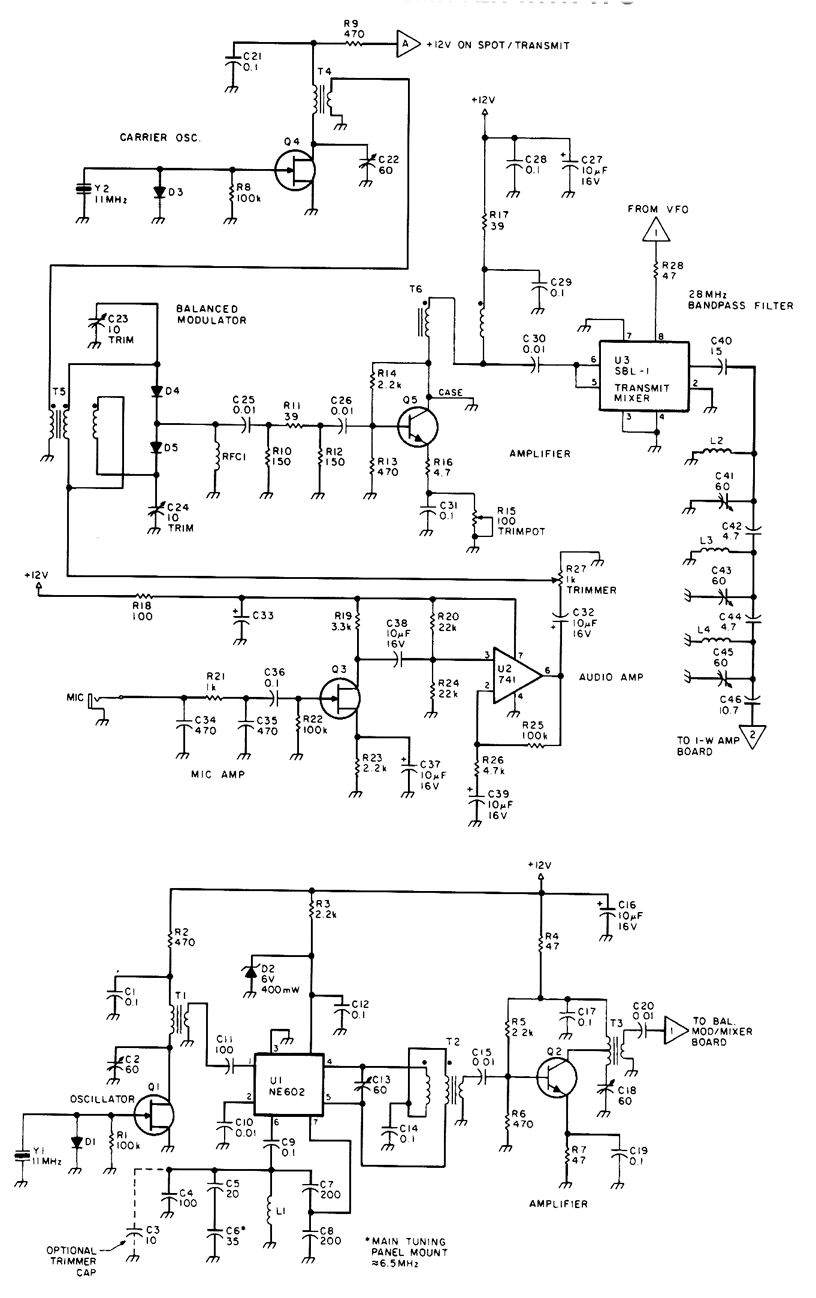
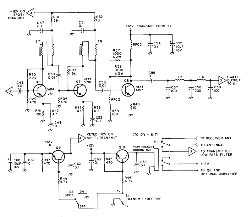
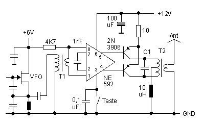
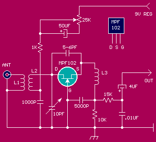
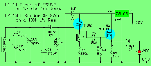
The circuit diagram shown in Figure illustrates the schematic for the 80/40 Meter Direct Conversion Receiver. A dipole or suitable antenna is fed directly to input jack J1, which is coupled to potentiometer R1, which serves as a continuously variable RF attenuator and also serves as the receiver’s gain control. Using the RF gain control to set volume is advantageous as it also reduces strong in-band signals that could otherwise overload the receiver front end. Series inductors L2 and L3, and trimmer capacitor C18, provide front-end bandpass filtering, and an impedance match to 50 to 75-ohm antenna systems. IC U1 is an NE602/612 mixer and Local Oscillator (LO) in an 8-pin dip package. The mixer section is an active Gilbert cell design for good conversion gain and low noise figure. The LO section uses heavy capacitive loading to minimize frequency drift. Tuning is capacitive, using a modern Hi-Q miniature plastic variable. The local oscillator (LO) stability is enhanced by a 78L05 voltage regulator. Since this is a direct conversion receiver, the LO is tuned to the carrier frequency of Single Sideband

Signals, or to a difference of 300 to 800 Hz on CW signals, to produce an aural output that is differentially coupled to a LM386 audio IC. The audio amplifier IC is coupled to the headphone jack at J2 by capacitor C16. The receiver circuit is power from a single 9 volt

transistor radio battery. Let’s get started! Before we begin building the 80/40 meter receiver, you will need to locate a clean well lit and well ventilated work area. A large table or workbench would be a suitable work surface for your project. Next you will want to locate a small 27 to 33 watt pencil tipped sol “Tip Tinner,” a soldering iron tip cleaner/dresser, from your local Radio Shack store. You will also want to secure a few hand tools for the project, such as a pair of small end-cutters, a pair of tweezers and a pair of

needle-nose pliers. Locate a small Phillips and a small flat-blade screwdriver, as well as a magnifying glass to round out your tool list. Grab the schematic, parts layout diagram as well as the resistor and capacitor identifier charts and we will begin our project. Place all the project components on the table in front of you. The 80/40 direct conversion radio is an RF or radio frequency project and it is best constructed on a printed circuit board with large ground plane areas covering the board for the best RF grounding techniques. Once you have all the parts and PC board in front of you, heat up the soldering iron and we’ll get started! First, find your resistor identifier chart in Table , which will help you select the resistors from the parts pile. Resistors used in this project are mostly small 1⁄4 watt carbon composition type resistors, which have colored bands along the resistor body. The first color

band should be closest to one end of the resistor body. This first color band represents the first digit of the resistor value. For example, resistor R2 has four color bands, the first one is a brown band followed by a green band followed by a black band. The fourth band is gold.

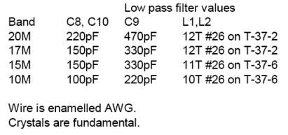
Note that the receiver can be built for either the 80 meter ham band or the 40 meter ham band. You will need to look at the parts list when deciding which band you want to receive. The inductors L1, L2 and L3 as well as capacitors C3, C4 and C5 determine the band selection.

This receiver project uses a number of small inductors. These small inductors will generally have color bands on them to help identify them. Molded chokes appear, at first glance, to be similar to resistors in both shape and band marking. However, a closer look will enable you to differentiate between the two––chokes are generally larger in diameter and fatter

at the ends than resistors. When doing your inventory, separate out any chokes and consult the parts list for specific color-code information. Note, that inductor L1 is an adjustable slug tuned type. Remember that specific chokes are used for each band: see parts list before mounting the chokes. Chokes do not have polarity so they can be mounted in either direction on the PC board.

The 80/40 meter receiver utilizes two integrated circuits and a regulator IC. Take a look at the diagram shown in Figure, which illustrates the semiconductor pin-outs. When constructing the project it is best to use IC sockets as an insurance against a possible circuit failure down-the-road. Its much easier to unplug an IC rather than trying to un-solder it from the

PC board. IC sockets will have a notch or cut-out at one end of the plastic socket. Pin one (1) of the IC socket will be just to the left of the notch or cut-out. Note that pin 1 of U1 connects to C1, while pin one (1) of U2 connects to C15. When inserting the IC into its respective socket make sure you align pin one (1) of the IC with pin one (1) the socket. Failure to install the IC properly could result in damage to the IC as well as to the circuit when power is first applied.

clip_image004

Let’s finish the circuit board by mounting the volume control and the adjustable capacitors. The volume control potentiometer at R1 is a right angle PC board mounted type, which is placed at the edge of the PC board as is the main tuning capacitor. Capacitor C18, which is connected at the junction of L3 and C1, is an 8.2 pF trimmer type; go ahead and solder it to the circuit board using two pieces of bare #22 ga. stiff single conductor wire.

Locate main-tuning capacitor C19, now locate the mounting location for main tuning capacitor C19. The tuning capacitor was mounted on its side using doublesided sticky tape. Remove the protective cover from the double-sided tape, and firmly press the body of capacitor C19 to mount it to the PC board. Firmly press the double-sided tape over the silk-screened outline for the body of C19. You may decide to mount the tuning capacitor in a different way. At the rear of the capacitor: locate the four internal trimmer capacitors, and using a small jeweler’s screwdriver or alignment tool, fully open (unmesh) all four trimmers. Note: tuning shaft faces front of board. Bend the two rotor lugs so they are parallel to the front face of the capacitor as shown above.

Connect the two rotor lugs to the PC board ground points as shown using scraps of lead wire trimmed from resistors as jumper wires. Cut a 6′′ length of 24-AWG insulated hook-up wire in half. Remove about 1⁄4′′ of the insulation from each of the cut ends. Solder the jumpers to the capacitor rotor lugs, and to the ground foil run on the bottom of the PC board. Since the tuning capacitor has four sections, you can increase the tuning ranges by paralleling different sections to give a greater tuning range: see Table 9-3. If you used just the 140 pF section, your tuning range would be 190 kHz, but if you combined the 140 pF section with the 40 pF section your tuning range would become 180 pF and so forth. Capacitor jumpers: 180 pF = use 140-pF and 40-pF sections paralleled; 222 pF = use 140-pF and 82-pF sections paralleled; 262 pF = use 140-pF, 82-pF and a 40-pF sections paralleled; 302 pF = use all four capacitor sections in parallel

clip_image006

clip_image008

clip_image010

clip_image012

VWN homebrew QRP TX

VU2JMX@BANGALORE

My first homebrew QRP TX was a simple solidstate CW transmitter using SL100, SK100 and BD139 giving about 5Watts on 40 Mtr band. This circuit was popular in South India and was known as ' VWN' circuit.

  • A RFC similar to the one used in the VFO circuit is used in SK100 collector to ground end.
  • BD139 Tank coil is 4.4 uH and is wound with 24 swg enameled copper wire on a piece of polythene pipe of 1.7 cms OD & lenght 3 cms. Tap at 13th , 15th  and 16th turns. 13th tap can be used for 50 Ohms coax/ inverted 'V' Ant or 15th tap can be used for 75Ohm coax/ Dipole Ant.
  • Mount BD139 on a heatsink.
  • Keep input current (BD139) at less than 200mA.

VHF Regenerative Receiver


Submited By Nadisha 4S7NR

Looks very simple. But need bit experiance to build this receiver. It can be tuned from 140 to 150 Mhz covering the whole 2m band. This has a Super Regenerative detector. When properly tuned and aligned the receiver is very sensitive. The original author R.H.Longden writing in a Practical Wireless artical says that he could hear transmissions of 10 miles with a 6 inch wire antenna.

Receiver must be enclosed in an metel box and Tuning spindle should be fixed with a plastic knob. One should never try to construct this on IC boards or Vero boards.

L1 and L2 Coils should be wound using 18 SWG wire and L1 is only one turn where L2 has 4 turns (7/8 inch long). They are air wound on 1/2 inch diameter form. L2 should be next in-line to L1. Changing the turn spacing of L2 change the frequency. So you will have to experiment and find where it tunes. If you have an signal genarator - with in no time you will be in the business. L3 is not very critical, it has 30 turns of 26 SWG wire on a 1/4 inch diameter air core.

Once evry thing is okay, connect an audio amplifier, similer to LM386 and a sutable antenna to the receiver. Turn the 25k pot (Regen Control) where a strong hiss begins. This is roughly the correct posision. This hiss should cease when any signal of sufficiant strength is tuned in. Tune the 10pf tuning cap to search any stations or tune your signal genarator to see where the receiver is tuned. Once you know the place, adjust the coil. To increase the frequency, you will have to stretch the turns of L2.

http://www.qsl.net/qrp/rx/vhf-rx.htm

THE PIPPIN 40m TX


Found in the Web Page of G3PTO

The authot of the Pippin is G.M.King G3MY. Basically, it is a conventional Colpitt type crystal oscillator but with the output taken from a low value collector load resistor and direct coupling is made into the base of the PNP device used as an amplifier. The result is a circuit even more simple than the OXO and with considerable advantages.

The small amount of forward bias developed for the PA stage makes it very much easier to drive but is less than the voltage required to actually bias the stage "ON". Keying is in the emitter circuit of the oscillator stage and when the key is up and no current is being drawn there is no forward bias at all on the PA stages.

Pippin TX

The isolation of the PA from the oscillator by taking the drive from the low value oscillator collector load, is most impressive and there is virtually no pulling of the oscillator even if the PA load is briefly shorted to ground.

Input to the PA stage runs at 120 to 150mA. at 12 to 14 volts and output on 7Mhz runs at better than 1 watt measured into a 50 ohm load. The PA transistor has a "Stove Pipe" heat sink attached and has been left running continously for more than 1 hour without any complaint from the PA stage.

The collector choke is the usual type and uses 6 turns of 29 swg on two ferrite beads in tandem. The low pass filter infomation were not available in the Orginal artical. (4S7NR).

http://www.qsl.net/qrp/tx/pippin.htm

The Tuna Tin 2 Transmitter


by Doug Hendricks, KI6DS

I remember 1976 well. It was the 200th anniversary of our country, and there were celebrations everywhere. I also remember it as the year that I was first licensed as a Ham, with the call WB0YVK in Kansas. One of the other things that I remember about 1976 was a very famous article that appeared in QST. It was Doug DeMaw's "Tuna Tin 2" QRP Transmitter construction article in the May issue.

Tuna - Tin TX

The first thing that I decided to do was to update the circuit so that it could be reproduced with todays parts sources. Dave Meacham, W6EMD, is the technical advisor to the club (NorCal), and I contacted him for his help in translating the information. Dave very graciously provided me with the information on how to change the coils to components available today. Next, I decided to redo the board layout to fit the components. I built the circuit, it works great, and this article is the result. Here are the only component changes that need to be made to those in the original article.

5WATT TRANSMITTER


By Harry Lythall SM0VPO

This is a very simple 5 watt CW TX based upon a TTL logic chip. There is just one "tricky" component and this is Cx. This component should have an impedance of about 10 - 50 ohms, at the frequency of interest. If you wish to reduce the transmitter power, increase the value of Cx. It is 'Cx' which causes the square wave from the output transistor to approximate a sine wave. The value of Cx is the price of simplicity in this TX.

STARTING values for Cx are as follows
(but there is a LOT of leeway):

1.8 MHz = 4.7nf
3.5 MHz = 2.2nf

7.0 MHz = 1.2nf
10 MHz = 820pf

14 MHz = 560pf
18 MHz = 470pf

24 MHz = 390pf
28 MHz = 330pf

It is far better to use too high a value for Cx initially, then reduce it to achieve the correct RF output power. The value of Cx will depend upon your choice of TR1. Virtually any RF power transistor will work well in this application as long as it will handle 800mA continuously. I have even used the BC108 in this application but the RF power output was restricted to about 150mW. Cx was about 5x the value quoted above.
The output tuned circuit uses a coil WITHOUT a ferrite slug. Use the usual "rule-of-thumb" formula for the tuned circuit;

Coil
Wavelength (in meters)
=
number of turns

Capacitor
Wavelength (in meters)
=
Capacitance (pf)

This will get you 'roughly' in the right area although it could differ widely with different coil formers. The coil output winding is from 5% to 15% of the total number of turns. Adjust the output winding before reducing the value of Cx. You need the least number of turns that will give you the power needed.
Connect + 5 volts to the SN7400 chip and + 12 v to the PA and you will have over 5W of power out. To key the TX put the key in the +12v lead.
You MUST use an antenna Low Pass filter with this rig if you are using a good antenna. If the antenna is tuned (magnetic loop/frame antennas etc) then you need not bother with the LP-filter. Do NOT use a linear amplifier for this transmitter. The finished transmitter will fit into a matchbox with a little care.

VU2VWN's 7 on 7 Qrp


Submited By Nadisha 4S7NR

This is a VFO control, easy to build 7 watts QRP on 7 Mhz from Vasantha VU2VWN. If you are in close VU, you may hear hundreds of hams using this QRP on 7MHz - AM. They just modulate the whole Driver/Amp section using a Audio transfomer. It is very populer (specially) in South India.

VFO works with two MPF102 FEts. It should be enclosed. Many VU hams put this VFO on a Card-Bord box and wrap it with Aluminium foil. And they oparate the VFO using 6V battery and 5.1v Zener diode. I change it with 7805 three pin voltage regulator and still works okay (I mean with out any hum).

BD139 should be mounted on a large heat sink. Once everything is finish, Supply 12v to the Amp (not 24v) connect a 24v 5W bulb as the load. C4 should be tuned to the minimum brightness of the LED. Total DC current to the RF amp should be 200-300 and it should never exeed 400mA (at 12V). On its full power 28V power amp will take about 300-400mA (max 500). Use 75 ohm coax, to feed the dipole.

A sensitive RF probe

A sensitive RF probe is very useful in a situation where an oscilloscope is not available. This design allows measurement of the peak-to peak amplitude of an RF signal in the 100 kHz to the VHF range at up to 50 volts P-P. 50 Volts P-P is approximately 14 volts RMS. The 50 volt P-P limit is due to the 60 volt breakdown rating of the diodes

The upper frequency range limit of the probe is due to the length of the ground wire and the stray junction capacitance of the germanium diodes. It is designed for use with a high impedance DC voltmeter, or VOM. Instruments with FET inputs are preferable.Avoid using a long ground lead. Keep the ground lead as short as possible, and attach it as close as possible to the ground point of the circuit under test.

A thirty-six (36) inch length of RG-174 coax is recommended for the probe’s cable. RG-174 is well suited for this task because of its small diameter and flexibility. Also, #16-#18 guage insulated stranded hook-up wire can be used. Twist the wires together.

The RF probe is a charge pump. The peak crest value of a signal is stored in the stray capacitance of the coaxial cable. The stray capacitance of the cable is about 50 pF. The 50 pF capacitance of the cable, and the 10 mega-ohm input impedance of an FET VOM implies a DC filter time constant of 500 m Seconds, Accurate measurements are possible at frequencies as low as 100 kHz.

Noticeable errors occur at low signal levels because of the forward bias drop of the diodes. Assume a total diode voltage drop of about 0.3 volts.If a standard 20KW /Volt meter is used, then you may have to add a 1000 pF capacitor across the input of the VOM to improve DC filtering. Expect more circuit loading effects, and an increase in the probe’s lower cut-off frequency.

Modulation Transformer for QRP AM transmitter projects

One the stumbling block for QRP enthusiasts, interested in building AM transmitter related projects is need of modulation transformer. I have simple solution for this. You can use audio output transformer from old radio receivers.

modulation-transformer

Low Cost ATU for QRP rigs

image

The circuit shows simple low cost ATU for QRP transmitter projects. The coil is wound on a 12mm ferrite rod, which can be junked from old radio receivers.The wire will be 20swg and  the winding should occupy 4cm long.VC1 and VC2 are 365 pf Variable condensers used in radio receivers.